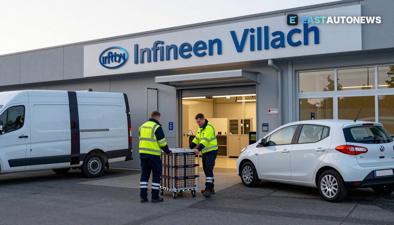
Infineon Technologies announced on 9 November 2026 that it has processed functional power devices on 300‑millimetre silicon‑carbide (SiC) wafers at its Villach, Austria semiconductor plant — the first demonstration of 300 mm SiC devices in a full‑scale fab environment. The company said the result shows the feasibility of moving SiC from smaller research wafers into a manufacturing context and will be presented at the electronica trade show in Munich on 10–13 November.
Technical milestone and company view
Infineon said a 300 mm SiC wafer offers about 2.3 times more chips than a 200 mm wafer, improving potential economies of scale for power devices used in electric‑vehicle traction inverters, on‑board chargers and charging infrastructure. The company added that the demonstrator was processed using existing silicon manufacturing equipment at Villach.
Jochen Hanebeck, Infineon’s CEO, called the work a step that “further strengthens our leadership in power systems.” The press release made clear Infineon will plan ramp timing with customers while continuing its 200 mm SiC roadmap.
What this means for the market
SiC devices are critical to EV efficiency and fast charging. A scalable 300 mm SiC process could reduce unit costs and raise output capacity for automakers and tier‑1 suppliers across Central and Eastern Europe that rely on European and global power‑semiconductor supply chains. Infineon explicitly highlighted automotive traction inverters, EV chargers and large energy‑storage converters among target applications.
For the region, two effects matter most: better supply security and lower long‑run component costs. Carmakers in CEE — from legacy European OEMs to new Chinese entrants building or sourcing in Hungary, Slovakia, Poland and Romania — face tight competition for SiC parts. A viable 300 mm SiC route at Villach, if industrialised, would add EU‑based capacity nearer to vehicle assembly and power‑electronics suppliers.
Infineon also reported it has proofed a related wafer‑separation process (Cold Split) for 300 mm SiC at its Dresden site and separately is investing about €1.1 billion in 300 mm gallium‑nitride (GaN) power production in Villach — moves that together underline a push to scale wide‑bandgap power chips in Europe. Those announcements signal to automotive procurement teams that more local semiconductor capacity is being targeted by a major IDM.
Near‑term caveats remain: Infineon’s statement is a technological demonstration, not a commercial‑volume ramp. The company did not give a specific mass‑production date, customer names or initial yields in the press release. Automakers and suppliers will watch ramp timing, yields and unit costs before altering sourcing strategies.
WorldTrader24 B2B-Fahrzeugmarkt für Händler →
Sources: Infineon Technologies, Electronic Design